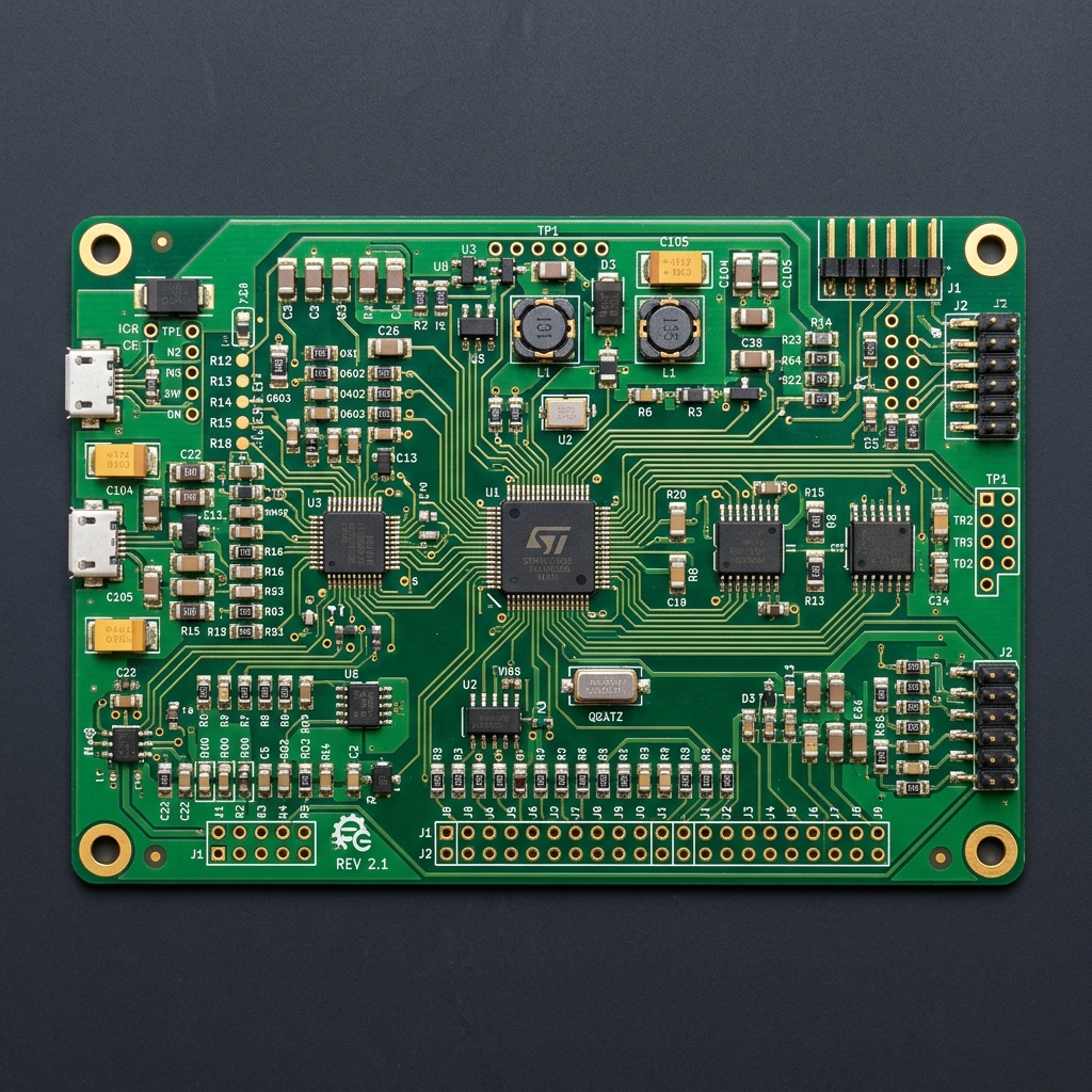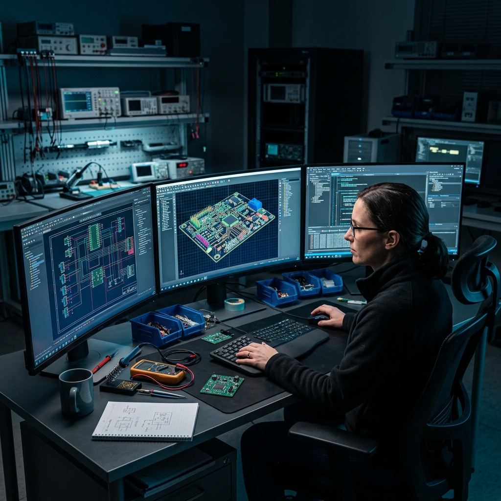
Advanced PCB CAM, PCB Design, PCBA, and Reverse Engineering Services
for Modern Electronics Companies Worldwide.
Nuva Circuit is a leading PCB CAM engineering and electronics manufacturing services company dedicated to delivering high-precision engineering solutions to electronics companies worldwide. We bridge the gap between design intent and manufacturing reality.
Rapid processing without compromising quality, meeting your tight production timelines.
Industry-standard compliance with IPC, IEC, and customer-specific requirements.
Dedicated technical support team available to assist throughout your project lifecycle.
Latest EDA software and CAM tools ensuring cutting-edge design and manufacturing output.
End-to-end PCB engineering support from design to manufacturing — built for precision, speed, and reliability.
Expert CAM processing for manufacturing-ready outputs. We handle every detail from raw design data to final production files.
Comprehensive PCB layout and schematic design services for complex, multi-layer, and high-speed applications.
Full-spectrum PCB assembly solutions with SMT and THT capabilities, combined with stringent quality inspection protocols.
Accurate PCB cloning and circuit analysis services to recreate discontinued or proprietary board designs with full documentation.
Trusted by electronics companies across the globe for our unwavering commitment to precision and delivery.
Sub-micron accuracy in CAM processing and layout design, adhering to the tightest industry tolerances.
Optimized workflows and 24/7 operations ensure your project ships on time, every time.
Engineers with deep domain knowledge in advanced PCB technologies, HDI, flex, and RF designs.
Multi-stage quality control and DFM verification to eliminate defects before they reach production.
Dedicated project managers and responsive communication channels keep you updated at every step.
Fully digital, cloud-supported engineering workflow with automated validation and revision control.
A streamlined, transparent workflow from your first requirement to final delivery.
Client shares design files, specifications, and project requirements with our engineering team.
Schematic capture, PCB layout, and design optimization by senior engineers using advanced EDA tools.
Comprehensive DFM checks, Gerber validation, and tooling optimization for manufacturing readiness.
Precision PCB fabrication and assembly using industry-standard equipment and materials.
Rigorous AOI, electrical testing, and final inspection to ensure zero-defect output.
Secure packaging and worldwide shipping with real-time tracking and full documentation.
Our precision engineering solutions serve a wide spectrum of high-technology industries worldwide.
Smartphones, wearables, smart home devices, and personal computing solutions.
ECUs, ADAS systems, infotainment, and EV battery management electronics.
PLCs, motor drives, robotics controllers, and factory automation systems.
Connected sensors, edge computing modules, smart meters, and M2M devices.
Patient monitoring, diagnostic equipment, imaging systems, and implantables.
5G infrastructure, base stations, RF modules, and network switching equipment.
Tell us about your PCB engineering requirements and we'll get back to you within 24 hours.
Ready to discuss your project? Our engineering team is available to help.